This article was originally posted on PinballRehab.com.
Reproduced with permission from terryb.
Written by terry
This is part four of a seven part series intended to provide a basic knowledge of electronics, test equipment, pinball manuals and troubleshooting in order to allow the reader to effectively repair pinball games. With that goal in mind I have simplified the explanations and purposely glossed over some details that add no value, and can easily confuse beginners.
Digital and Analog Circuits
A. Basic Electronics
B. Transistors
C. Integrated Circuits
D. Test Equipment
E. Operators Manual
F. Reading Schematics
G. Electronics Troublshooting
A digital circuit is like a light switch, it is either on or off. Although, like a strobe light, it can be switched on and off very quickly.
Digital circuits have two logic states. They are either low (represented as binary 0) or high (represented as binary 1). In addition a circuit can alternate between low and high ( a pulsed circuit). While low/high circuitry can be troubleshot with a DMM, you really need a logic probe, or oscilloscope, to effectively repair pulsed circuits.
Analog circuits have variable and proportional (more on that later) inputs and outputs (like the volumn control on a radio). Because of the range of outputs available (rather than just a 0 or 1), analog circuits are typically used for audio and video. Analog circuits are more difficult to troubleshoot.
Logic Families
There are different logic families, or generations, of integrated circuits. Each logic family has different behavior and within each logic family there can be subsets with different characteristics. The only two we need to be concerned with in regards to pinball are TTL and CMOS. TTL chips are used in digital circuits while CMOS chips can be used in analog or digital circuits.
Note: The information in this section has been simplified in order to align with the goal of a beginner level guide. For example, a TTL gate has different input and output logic levels although we will consider them as being the same. This is also true for a CMOS gate, and the values provided below are the input voltage ranges for TTL and CMOS. If you want to fully understand the differences between TTL and CMOS logic levels see the Logic Signals Voltage Levels article at All About Circuits.
TTL chips use a nominal Vcc (Vcc is the fancy term for the supply voltage) of 5 volts and the inputs and outputs are always binary (low, high or pulsed). TTL chips typically use a standard naming convention of 54XX or 74XX. On the other hand, CMOS chips can use a Vcc ranging from 3 – 15 volts and depending on the chip can have either binary or analog inputs and outputs. CMOS chips typically use a numbering convention of 40XX or 45XX.
One example of CMOS in a pinball is the LM339 voltage comparator chips used in Williams/Bally switch optic circuits.
Based on the logic family of the chip there are different voltage ranges that are considered to be low or high in a digital circuit. In the case of TTL the low range is 0 – .8 volts and the high range is 2 – 5 volts. So any reading between 0 and .8 volts is considered a logic 0 and any reading between 2 and 5 volts is considered a logic 1.
The specification for CMOS circuitry in a 5 volt circuit is a low range of 0 – 1.5 and a high range of 3.5 – 5. For a 10 volt Vcc the low range would be 0 – 3 volts and the high range 7 – 10 volts. The high and low voltage ranges scale linearly across the possible supply voltages of 3 -15 volts.
Because of the difference in voltage ranges for high and low between TTL and CMOS they are generally not intermixed in the same circuit, and when they are additional circuitry is required to match up the logic levels. Although there is a subset of CMOS (numbered 74HCTXX) that uses TTL input voltages and a 5 volt Vcc.
Logic Gates
A logic gate is a physical device that uses Boolean logic (more on this later) to perform a logical operation on one or more logic inputs and produces a single logic output. The following diagram shows the basic logic components and their outputs based on various inputs (a binary 0 equals low and a binary 1 equals high).
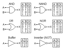 First we’ll discuss the AND gate. The AND gate requires both inputs to be high in order to produce a high output. If either input is low, the output will be low. The Boolean formula for an AND gate is A * B = X.
In the case of an OR gate if either input is high the output will be high.
If you look at the NAND gate and the NOR gate you’ll notice a small circle on the output. The easiest way to understand these gates is to consider it like two components. The first part works the same as a normal AND gate and the second part, the circle, is an inverter. An inverter flips the output; so low becomes high and high becomes low.
If you compare the outputs between an AND gate and a NAND gate you will notice they are the opposite. The AND gate portion of the NAND gate works the same but the inverter flips the output.
Our next two gates are pretty simple. A buffer outputs the same voltage as the input and an inverter flips the output (note the circle, which works the same as described above).
Keep in mind that for all types of gates, if the input is pulsed, the output will be pulsed (if the other logic requirements are met). So in the case of an AND gate with A = 1 and B = pulsed (alternating 0 and 1), when B is high the output will be high and when B is low the output will be low. In other words, the output will be pulsed. On the other hand if A = 0 and B = pulsed the output will be 0 since the AND logic requirement of two high inputs is not met. When there is a pulsed input it will typically only be one of the inputs, not both.
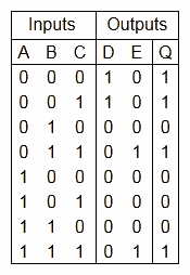
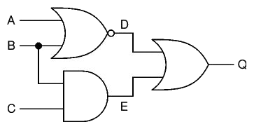 Time for a little summary using the circuitry to the right with the following inputs: A = 0, B = 1 and C = 1. In the top left we have a NOR gate (notice the inverter) with inputs of 0 and 1. So an OR gate would have an output of 1, but it is inverted, so in our example D = 0. Below the NOR gate is an AND gate with inputs of 1 and 1. This one should be easy, E = 1. Our last gate to the right is an OR gate with inputs (D and E) of 0 and 1, therefore our output would be 1.
Try a few more examples on your own with A, B and C inputs of 0 1 0 or 1 0 0 or 1 0 1 or any other combo you like. The answers are at the bottom of this article.
Analog Circuits
As mentioned earlier, CMOS chips are used in analog circuits and the inputs and outputs are variable and proportional. For example, consider a 7404 inverter (TTL). If the input is low, the output is high and if the input is high the output is low. The functionally equivalent CMOS chip is a 4069 inverter, but it works quite differently.
Because it works with ranges of voltage instead of only low and high the output is gradually increased or decreased in inverse proportion (because it’s an inverter) to the input. For example, if the operating voltage is 12 volts and the input is 4 volts, the output will be 8 volts. If the input is 8 volts, the output will be 4 volts.
Packaging
 Transistors typically have a one-to-one relationship between the schematic and the circuit board. In other words Q30 on the schematic is a single device on the board. In the case of logic gates, multiple gates are combined into a single chip (also called an IC or integrated circuit).
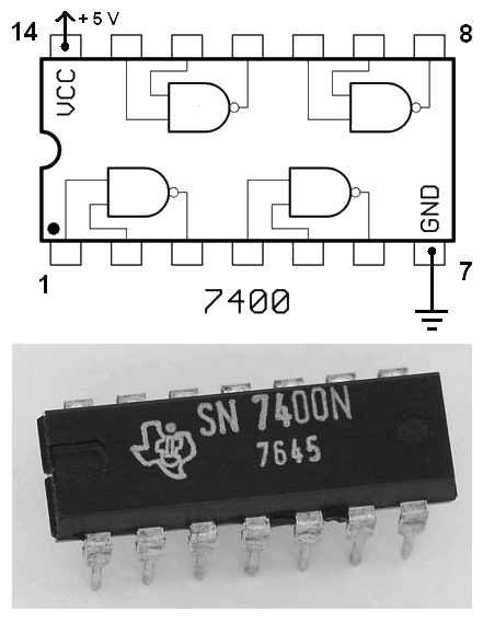
The image to the right shows the layout of a 7400 Quad NAND chip. So while this is one physical device, on the schematic it will be shown as four separate NAND gates, each operating discretely from the others. Each gate that is part of the same chip will have a letter after the IC designator (for example, 18A, 18B, 18C and 18D).
The first question when troubleshooting is, which is pin 1 and how are the pins numbered? Firstly, pins are always numbered counter-clockwise starting with pin 1, which can be identified in two ways depending on the manufacturer. The first method uses a small dot, or recessed circle, placed next to pin 1. The second method is a semi-circle placed on one end of the chip with pin 1 being the first pin counter-clockwise from the semi-circle (see the image to the right).
Some chips will use both methods, and for some reason some chip manufacturers place a circle in the middle of one end of the chip, usually opposite the semi-circle. This circle means nothing, so ignore it. You can see various examples of these markings in the first image in this article (hint: pin 1 is in the upper right hand corner on every chip in the photo).
Other than ASIC’s, pin 1 is always a corner pin. On ASIC’s, pin 1 is in the middle of one side and marked with a circle.
On 14 pin chips, pin 7 is always ground and pin 14 is always Vcc. On other chips you can use an ohmmeter to identify the correct pins by testing connectivity between the pins and the ground and Vcc test points on the circuit board. Note that if you put a chip in backwards, pin 7 would be connected to Vcc and pin 1 to ground. This is both possible to do and results in bad things happening.
The pin 1 location is usually indicated on the circuit board either with a silk-screened rectangle with a notch or a number 1 for pin 1. When there’s a a chip socket it will have a notch matching the notch on the chip. In either case it’s still a good idea to note the chip orientation when removing it.
Testing Logic Chips
The best way to test chips is in-circuit with power, which is covered in the Repair Guides section of our site. A less accurate, but sometimes effective way is using an ohmmeter. Be aware though this method will not identify all types of failures and works much better if the chip is removed from the circuit, which is often not a good option.
Put your DMM in diode mode and place the red lead on the ground pin. Put your black lead on each of the other pins, except Vcc, and you should get a reading of .4 to .6. Again, this is not the best way, but sometimes helps in a pinch.
A better method is using a chip tester, although they are expensive and require the chip to be removed from the circuit.
[Editors note: See the section on using Digital Logic Probes for additional testing information.]
LM339
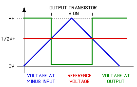 The switch matrix circuit use an LM339 chip, which is a quad comparator (there are four voltage comparators in the package). The output of an LM339 switches on or off depending on the relative voltages at the plus and minus inputs of the comparator. The inputs are quite sensitive and a difference of only a few millivolts between them will cause the output to change (see image to the right).
Current will flow through the collector when the voltage at the plus input is lower than the voltage at the minus input. Current will not flow through the collector when the voltage at the plus input is higher than the voltage at the minus input.
If you want to learn more see the following article Voltage Comparator Information and Circuits or the LM339 Datasheet.
74LS374SC
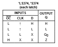 By using Boolean logic an IC can be setup to have memory (this is how RAM chips work). By feeding the output of a gate back into the input, the gate will remember the input value. This type of IC is commonly called a flip-flop.
The LS374SC chip is an edge-triggered D-type flip-flop. When the clock transitions to positive, the logic states at the output (Q) are set to the same value as the input (D) as long as a clock cycle is present (see image to the right for the Boolean logic).
The 374SC inputs are typically connected to the data bus. An example of this in a pinball game is the switch-matrix circuit where is is used to provide a constant pulsed signal to the column side of the circuit.
You can learn more about flip-flops at Wikipedia or in the LS374 Datasheet.
Buffers
Input/output circuits process data to and from other boards (video, sound, etc.) and use buffers to prevent cross-talk and interference. There are two basic types of buffers: unidirectional and bi-directional. While unidirectional buffers pass data in only one direction, bi-directional buffers can pass data in either direction depending on the input to pin 1.
Buffers are used on the CPU board to control I/O output, and input in the case of bi-directional buffers, to other boards or circuits. Common buffers in a pinball game include 74LS240, 74LS244 and 74LS245. For more information, here’s the 74LS240 Datasheet (unidirectional) and 74LS245 Datasheet (bidirectional).
Peripheral Interface Device (PIA)
The following image shows a portion of a MPU/CPU pinball schematic including a PIA chip. While explaining thoroughly how PIA chips work is well beyond the scope of this article (and not really of much value) I do want to cover them briefly since they do occasionally go bad.
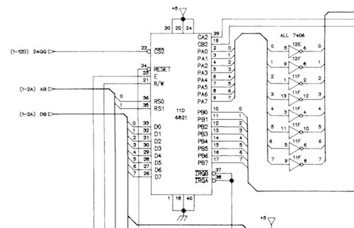 The PIA chip serves an important function as the point where the system’s processor interfaces with the logic circuits which we’ve previously discussed. In the example above the data lines (D0 -D7) receive information from the processor and send out control signals (PA0-PA7 and PB0-PB7) to the logic circuits and then the driver transistors which control lamps, flashers, solenoids, etc.
 If using one of our Repair Guides you’ve gotten to the point where the problem is either the PIA chip or something up-stream of the PIA chip the answer is rather easy to determine. If the PIA chip is getting bad inputs (either on the data lines, clock, reset, etc.) the machine will typically have multiple problems. For example, a single bad data line will affect multiple outputs.
If you are only wrestling with one problem, a solenoid that won’t fire for example, the inputs are probably all good and the chip itself is the problem.
Note: PIA chip problems will often, but not always, be indicated by the CPU diagnostic LED’s.
Logic Quiz Answers
Here are the answers to the logic quiz I presented earlier. If you haven’t already I really suggest you go through the various possible inputs and see if you can correctly identify the correct outputs. This is probably the most important portion of this document and will aid you immensely when troubleshooting circuit boards.
References
- The following is a great site that provides more in-depth electronic tutorials: All About Circuits.
- Randy Fromm’s YouTube Channel also has some great videos on basic electronics theory.
Comments
Comments, including general questions about electronics troubleshooting, suggestions, improvements, errors, etc. are welcome (see below).
If you have a specific question about your game, please see our FAQ section.