This article was originally posted on PinballRehab.com.
Reproduced with permission from terryb.
Written by terry
A. Basic Electronics
B. Transistors
C. Integrated Circuits
D. Test Equipment
E. Operators Manual
F. Reading Schematics
G. Electronics Troublshooting
This is part six of a seven part series intended to provide a basic knowledge of electronics, test equipment, pinball manuals and troubleshooting in order to allow the reader to effectively repair pinball games. With that goal in mind I have simplified the explanations and purposely glossed over some details that add no value, and can easily confuse beginners.
Whether you’re troubleshooting a circuit or testing your work after replacing an IC, knowing how to read a schematic is a necessity. While you don’t need to become a EE, you should be able to walk through a circuit and understand what components are involved and what connects to what. In addition, you should also be able to look at a schematic and correlate the component drawing to the physical device (see Image 1).
Understanding the function of individual components is a prerequisite for this article (see references). With that knowledge and the ability to read a schematic, you can break the circuit down into manageable chunks that can be analyzed and repaired.
Types of Drawings and Schematics
There are three common types of drawings/schematics you will be concerned with.
The first is a block, or logic, diagram. Image 2 is an example of a block diagram for the flipper and lane change circuit on Addams Family. A block diagram is a combined and simplified (only the flipper circuit is shown in Image 2) version of the wiring diagram and the appropriate schematics.


Next are schematics which provide complete circuit information for each board and in the case of some boards like the CPU are spread over multiple pages.
The last type of document is the wiring diagram which provides interconnect information between circuit boards and/or the playfield wiring.
Physical vs Logical
One of the things all beginners struggle with is correlating component drawings on a schematic (a logical representation of the circuit) to their counterparts on the board (a physical representation of the circuit). Most people when looking at a schematic tend to relate it to something they’re familiar with; a road map. Therefore the physical orientation and the scale is assumed to be accurate.
Unfortunately that’s not true.
Schematics are a logical representation of a circuit and have no correlation (other than coincidental or ease of manufacturing) to the physical representation of a circuit on a board.
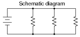
On the right is a simple parallel circuit with a power supply (battery) and three resistors. While you might think the three resistors will be located on the board next to each other in parallel, that isn’t necessarily true. In fact the resistors on the board might be laid out in series (remember what matters is the wiring, not the location).
Just as the physical orientation doesn’t matter, the distance between components doesn’t matter (technically in some circuits it does, but let’s ignore that point for now). In fact (although unlikely) our three resistors might be located on completely different parts of the board. A more realistic example, is the power supply, which could be located anywhere since it probably powers other circuitry.
The point is that not only does the schematic provide no indication of layout is also provides no indication of proximity. A long line on the schematic might be a short trace on the board, and a short line might be a long trace.
The last point is that since schematics are logical representations, there is not always a one-to-one relationship between the drawing of a component and the physical device. Luckily this only comes up on pinball games in a couple of instances.
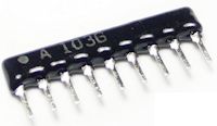
The first is resistor networks, which are a bundle of several resistors in one physical package (see image to the right). In some cases the resistors will be drawn as a bundle (see Image 10) other times they will all be drawn as indiviual resistors.
Integrated circuits have similar issues since most chips consist of multiple gates. For example, a quad AND gate has four internal AND gates, each of which will be drawn seperately on the schematic. This topic will be coverd in more depth later in this article.
Connectors and Wiring
Traces and wires are indicated on the schematic as lines. Intersecting lines do not indicate that two traces/wires are connected. It would be impossible to draw a complicated circuit without unrelated lines crossing each other on the schematic. In order to differentiate the two, connected traces are indicated by a dot at the point where the lines cross.
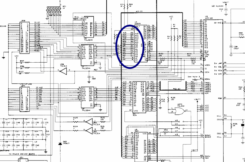
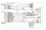
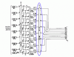
There are also times when multiple traces will be grouped together. This is common with address and data lines. The wires are not physically connected, but grouped in order to simplify the drawing (see Image 3). Address and data lines are also commonly connected to multiple devices.
Each end of the grouped wires (where they go to a component) will be individually labeled (i.e. – A0, A1, A2… for address lines or D0, D1, D2… for data lines) so you can follow the circuit.
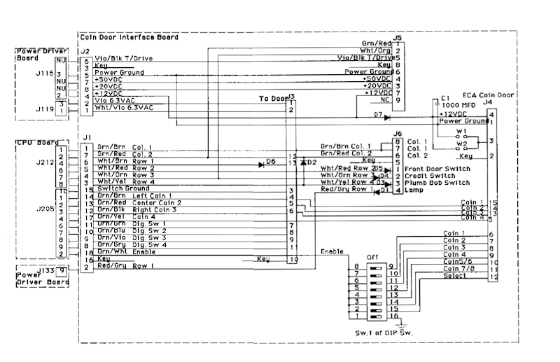
You will often need to work through multiple schematics by using the connector number and pin number to follow the wiring. Sometimes the drawing you are working with will show the second connector. Other times you will need to check the interconnect diagram to see where the wiring goes. In Image 4 you can see the interconnect wiring between the CPU and the coin door board.
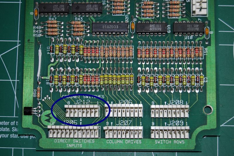
When looking at the board there will typically be a silk-screened number or arrow indicating which is pin 1. Be careful though because some boards will have a an arrow indicating the keyed pin (see Image 5). For a single row connector, the pins are numbered sequentially from the first pin. Keyed pins also have a pin number, so don’t skip them when counting.
On connectors with two rows, like some Molex connectors and most ribbon cables, pin 1 will be identified in the same way, but counting the other pins is slightly different. On a ribbon cable the pins will be numbered in pairs (see Image 6). Pin 1 is in the first row, pin 2 in the second row, pin 3 in the first row, pin 4 in the second row, etc.

Molex connectors are instead numbered sequentially across each row. For example, on a 20 pin connector, pins 1 through 10 are in the first row and pins 11 through 20 on the second row, with pin 11 next to pin 1.
One last thing to note about wiring is that while normally all wires labeled gry, for example, would be electrically the same, there are some exceptions. Since there is often not enough wire colors for all of the circuits, the same wire color is sometimes used on different circuits.
Normally, but not always, two wires with the same color code will be used on circuits that use a different gauge wire. For example, a yel-gry 18 gauge wire used as part of the switch matrix and a yel-gry 12 gauge wire used in the power supply. This is done purposefully to help avoid confusion.
Component Identifiers
Following are the common component designators. Each designator will be followed by one or more numbers which indicate the specific component. For example, the letter J is used for connectors and will use numbers like J116 to identify the specific connector.
- F is used for fuses.
- C is used for capacitors.
- R is used for resistors.
- BR is used for bridges.
- Q is used for transistors.
- U is used for IC’s.
Integrated Circuits
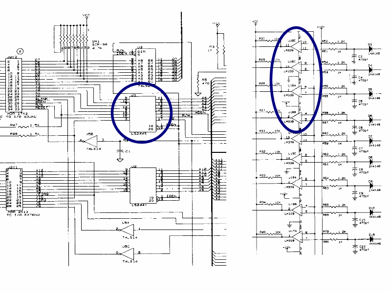
Integrated circuits can be shown on a schematic as logical or physical devices. Most simple IC”s (AND gates, inverters, etc.) are shown as logical devices. Other IC’s like RAM, game ROM and CPU are typically drawn as a physical device.
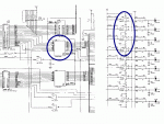
On the left in Image 7 I’ve circled U1, which is an LS244 buffer. In this case it is shown as a physical device and the only way to get more information on its internal configuration would be to look up the datasheet for an LS244.
On the right I’ve circled U18A-D, which is an LM339. In this case it is shown as four logical devices when it is actually one physical device (hence the A-D designation after the U18).
Other than ASIC’s, all IC’s use the same numbering method for their pins. The first pin is typically denoted by a screened or imprinted circle on one corner of the IC. The other pins are then numbered counter-clockwise from pin 1. Some chips will instead us a semi-circle at one end of the package. Pin 1 is the first pin counter-clockwise from the semi-circle.
In the case of ASIC’s, pin 1 is marked the same way but is in the middle of one side of the package.
Miscellaneous Info
A couple of other things worth noting on the schematics are the term Vcc and a series of 3 or 4 horizontal lines that form a small triangle pointing downwards (you can see both in Image 3).
Vcc is just a fancy name for supply voltage. The actual voltage at Vcc will vary depending on the circuit but will typically be either 5 volts or 12 volts. The triangle symbol represents ground.
Flipper Schematic

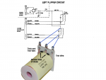
I constantly see requests on Pinside for photos of flipper mechanisms in order to verify wiring. Rather than trust a photo this is a great opportunity to start learning how to read schematics.
In Image 1 is a flipper schematic with three blue lines connecting to a photo of a dual-wound coil. The gry-yel wire goes to the outside coil lug with two windings, the blk-blu wire goes to the middle lug and the org-gry wire goes to the outside lug with only one winding.
The first diode is oriented with the band towards the outside lug with two coil windings and the second diode is installed with the band towards the middle lug.
Piece of cake right?
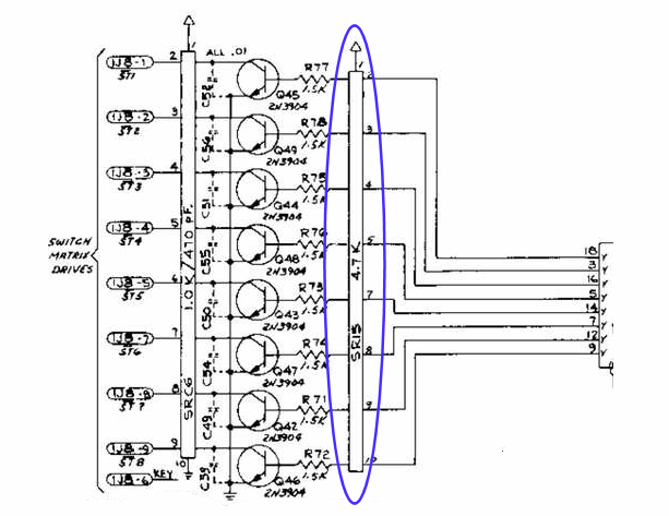
Switch Matrix Schematic

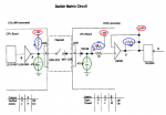
We’ll start with the generic switch matrix circuit logic diagram in Image 8. Although it does not provide the component identifiers for the specific circuit we might be concerned with it does provide a simpler view to start with. It also provides the various test point readings when the switch is open or closed. Note: These are pulsed circuits and best read with an oscilloscope or logic probe.
On the left is the column (also called send) circuitry on the CPU and on the right the row, or return side. In the middle is the playfield wiring, which connects to the board through J206 and J208.
Especially when first learning to read schematics it is easier to narrow your focus down to the key components. Every circuit contains standard components that serve a very basic function and rarely fail. In this case there are three pull-up resistors, which help provide a solid high signal (5 or 12 volts). There are also two capacitors that help moderate spikes when the circuit is switched.
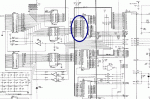
Once we eliminate the standard components you can see we have a basic serial circuit. Two chips on the send side and two chips, a diode and a resistor on the return side. You will also note that based on the Vcc (supply voltage) circled in red that part of each circuit is 12 volts and part 5 volts.
If you’ve read the earlier electronics tutorials you should know what purpose the remaining components serve. The ULN-2803 is an inverter (inverts the signal), The two diodes serve as blocking diodes (current can only flow through them in one direction). The LM339 is a voltage comparator, the LS374SC is a flip-flop and the 74LS240 is a buffer.
See Electronics Tutorial – Integrated Circuits in the references for more information on these IC’s.
Now we’ll move on to the schematic. When moving from one diagram/schematic to another it’s easy to get lost. Typically the best reference is the connector since it’s easy to locate on any drawing/schematic.
So if we we’re having a problem with row 1 you can see in Image 8 the connector on the CPU board is J208. In Image 9 I’ve pulled part of the CPU schematic where J208 is located, with row 1 highlighted. Note this is the same circuit as in Image 8 (other than being mirrored), but we now have the chip identifiers and pin numbers annotated.
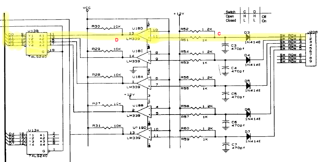
I have added the test points from the logic diagram to the CPU schematic. At this point you can walk through the circuit and take readings.
Note: It is not uncommon to need data from two different drawings/schematics, and IC or transistor datasheets, in order to troubleshoot a circuit.
Datasheets
There are cases, as above with the 74LS240, when all that is shown on the schematic is the physical device. In order to find out what the chip is actually doing you can get the datasheet for it, which is available online (just Google datasheet and the chip number). Most datasheets will also have a function table that will show what the output of the gate should be based on the various input possibilities.
Datasheets for transistors also provide additional information, especially on Darlington pairs, which comes in handy.
References
- The following is a great site that provides more in-depth electronic tutorials: All About Circuits.
- Randy Fromm’s YouTube Channel also has some great videos on basic electronics theory.
Comments
Comments, including general questions about electronics troubleshooting, suggestions, improvements, errors, etc. are welcome (see below).
If you have a specific question about your game, please see our FAQ section.